

Introduction
Crystal defects in epitaxial thin films may cause problems when producing high-performance semiconductor devices. Epitaxial thin films may inherit crystal defects from the single crystal substrate. It is important to evaluate the grains and crystal defects of the single crystal substrate before film growth on it. X-ray topography is an XRD imaging technique used to observe crystal defect distribution in a single crystal substrate. The SmartLab automated multipurpose X-ray diffractometer, equipped with an Xsight™ Micron FC high-sensitivity X-ray CCD camera, is capable of obtaining high-resolution topographs like those measured with dedicated equipment.
Measurements and Results
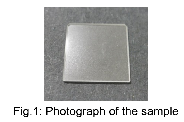
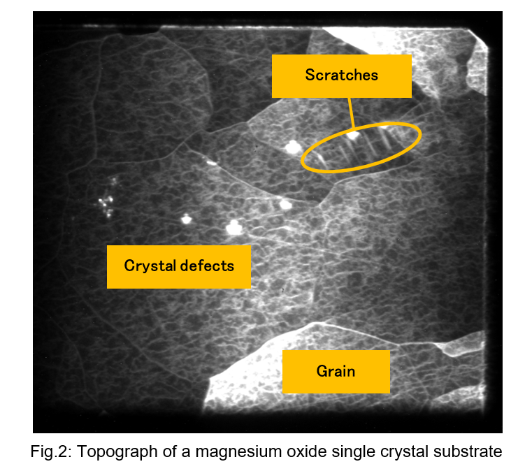
A 10 mm × 10 mm magnesium oxide single crystal substrate (Fig. 1) was observed by X-ray reflection topography (MgO 024 reflection, incident angle ω= 28.3˚, diffraction angle 2θ= 109.8˚, exposure time =120 sec.). Fig. 2 shows the obtained topograph. Grains separated by white lines, crystal defects shown as white spots or fine mesh patterns, and scratches were observed.
Recommended equipment
► Automated multipurpose X-ray diffractometer SmartLab
► High-sensitivity X-ray CCD camera XsightTM Micron FC
SmartLab
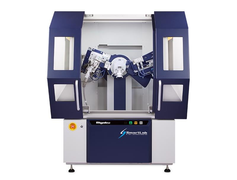
Automated multipurpose X-ray diffractometer (XRD) with Guidance software
